Why Do We Use Copper to Make PCB Traces?
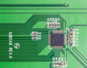
A printed circuit board (PCB) is made up of several layers, including the substrate, traces, soldermask, and silkscreen. The traces are a crucial element, because they carry the electrical signals to different components across the board. Without the traces, the PCB wouldn’t function. No PCB means almost every single electrical item that transfers data wouldn’t work!
Printed circuit boards (PCBs) have become a staple in virtually all areas of modern technology. Everything from smartphones to 3D printers makes use of PCBs, and the prevalence of PCBs in daily life is only going to increase. Of all the components that make up PCBs, copper is one of the most important.
The most common element used to make traces is copper. Why is copper such a popular choice in the PCB industry?
Why We Use Copper
 The number one benefit of copper is that it is highly conductive. This means that it can easily transmit signals without losing electricity along the way. It also means that manufacturers don’t have to use tons of copper. Even just a small amount will get the job done. In the most common configuration, an ounce of copper can be turned into 35 micrometers about 1.4 thousandths of an inch thick, which can cover an entire square foot of the PCB substrate. Copper is also readily available and relatively inexpensive.
PCBs rely on electricity in order to perform their myriad functions. The titular circuits in these circuit boards are essentially pathways that channel electric charges from one location to another, and the pathways must be able to carry the charges efficiently. While dozens of substances can carry electric charges, copper is particularly conductive, so it has become the standard choice.
The reason for copper’s high level of conductivity is that it has only one valence electron, also known as a free electron. Such electrons can travel freely from one atom to another with very little resistance. Electrons are the fundamental particles that hold electrical charges, so free electrons are responsible for transferring electrical signals. Copper transfers these signals without losing electricity.
Together, these factors make copper the ideal element to be used as PCB traces.
We provide a complete suite of PCB Assembly Services, including rework and modification, BGA, SMT, Turnkey, Thru-Hole, Lead Free, and Prototype assembly, plus an extensive line of add-on services, such as Injection Molding and Metal Work & Finishing.
Do you have more PCB questions?

