Printed Circuit Boards (PCBs) are the unsung heroes of the modern technological age. These seemingly unassuming boards are at the heart of almost every electronic device we use today, from smartphones and laptops to refrigerators and cars. Despite their ubiquity, PCBs often remain a mystery to many. This comprehensive guide aims to shed light on what PCBs are, how they work, and why they are so crucial.
What is a Printed Circuit Board?
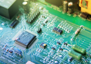
A Printed Circuit Board is a flat, typically green, rectangular board made from non-conductive material, usually fiberglass. The surface of the PCB is etched with thin lines of copper, creating pathways that connect various electronic components. These pathways, known as traces, allow electricity to flow through the board, enabling the components to communicate and function together.
Key Components of a PCB
- Substrate: The foundation of the PCB, providing its structure and rigidity. Made from materials like fiberglass, it ensures the board can withstand physical stress and high temperatures.
- Copper Layers: These are the conductive pathways that carry electrical signals between different parts of the PCB. Depending on the complexity, a PCB can have one or multiple layers of copper.
- Solder Mask: The green (or sometimes blue, red, or black) layer that covers the copper traces to prevent them from short-circuiting and to protect them from environmental damage.
- Silkscreen: The white markings on the PCB that provide labels and indicators for the placement of components. This layer helps engineers and technicians during assembly and troubleshooting.
Types of PCBs
PCBs come in various types, each designed to meet specific needs:
- Single-Sided PCBs: These have copper traces on one side of the board only. They are simple and inexpensive but limited in functionality.
- Double-Sided PCBs: These have copper traces on both sides, allowing for more complex circuits.
- Multi-Layer PCBs: These consist of several layers of copper separated by insulating material, enabling highly complex and dense circuit designs.
- Rigid PCBs: Made from solid, inflexible materials, these are used in most common electronics.
- Flexible PCBs: Made from flexible plastic substrates, these can bend and fold, making them ideal for applications where space is a premium.
- Rigid-Flex PCBs: A combination of rigid and flexible PCBs, providing a balance of flexibility and durability.
How are PCBs Made?
The manufacturing process of PCBs involves several precise and intricate steps:
- Design: Engineers use specialized software to design the layout of the PCB, ensuring that the electrical paths and component placements are optimized for performance and reliability.
- Printing the Design: The design is printed onto a photomask, which is then used to transfer the design onto the copper layer of the PCB.
- Etching: The PCB is exposed to a chemical solution that removes excess copper, leaving behind only the desired copper traces.
- Lamination: For multi-layer PCBs, multiple layers are laminated together under heat and pressure.
- Drilling: Holes are drilled into the PCB to allow for the placement of components and the creation of vias (pathways that connect different layers of the PCB).
- Plating and Coating: The PCB is plated with additional copper and coated with solder mask and silkscreen.
- Assembly: Components are placed onto the PCB and soldered into place, either by hand or using automated machines.
The Importance of PCBs

PCBs are essential for the functionality and miniaturization of modern electronic devices. They provide a compact and reliable means of connecting electronic components, enabling complex circuits to be implemented in small spaces. Without PCBs, the technological advancements we enjoy today would not be possible.
Understanding PCBs is crucial for anyone interested in electronics and technology. These boards are the backbone of modern electronic devices, providing the necessary connections and structure for components to work together seamlessly. Whether you’re a hobbyist tinkering with electronics or a professional engineer designing cutting-edge technology, a solid grasp of PCB fundamentals is invaluable.
By demystifying PCBs, we can appreciate the incredible ingenuity and precision that goes into creating the devices we rely on every day. So, the next time you use your smartphone or turn on your laptop, take a moment to think about the tiny yet mighty PCB inside, making it all possible.
CLICK HERE TO GET IN TOUCH
Yun Industrial has been providing Electronic Manufacturing Services (EMS) as a PCB Assembly House in the Los Angeles area since 1993.
We work for customers locally and across the country. We look forward to hearing from you!


