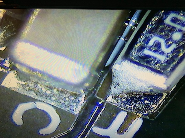
Wetting issues in PCB assembly can significantly impact the quality and reliability of solder joints. These issues are generally classified into two categories: Non-wetting and Dewetting. Both conditions can lead to defective connections and reduced circuit performance if not properly identified and corrected.
What Is Non-Wetting?
Non-wetting occurs when molten solder fails to bond with the base metal surface. During the reflow soldering process, if the solder cannot adhere to the PCB pads or the component leads, it results in incomplete or weak joints. This is often caused by oxidation, contamination, or inadequate heat, which prevents proper metallurgical bonding.
What Is Dewetting?
Dewetting happens when molten solder initially wets the surface but then recedes, leaving behind small, irregular mounds surrounded by thin solder films. Although the base metal is covered, the resulting joint lacks a full solder fillet, weakening its mechanical and electrical integrity. Dewetting is often associated with poor solderability of the PCB pad or component terminations.
Common Causes of Wetting Issues
Several factors can contribute to non-wetting or dewetting problems:
Oxidized PCB pads or component pins, preventing solder adhesion
Low soldering temperatures, especially with lead-free alloys
Expired solder paste, which leads to inactive flux
Thin plating thickness (less than 5 microns), reducing solderability
How to Fix or Prevent Wetting Problems
To minimize wetting issues during PCB assembly, follow these best practices:
Store PCBs and components in controlled environments (humidity and temperature)
Avoid using PCBs that have been in storage for over one year without protective covers
Remove oxidation by dipping the board in 2% sulfuric acid for 2–3 minutes before re-soldering
Always check the expiration date of solder paste before use
By maintaining strict process controls and quality standards, you can prevent wetting defects and improve overall solder joint reliability.
📞 Need expert PCB assembly or troubleshooting for wetting issues? Contact ACME PCB today for high-reliability assembly backed by decades of experience.


