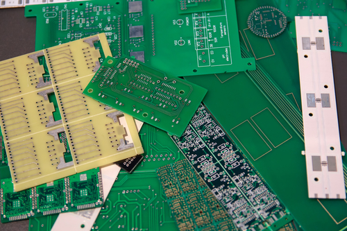
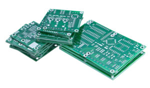
 Printed Circuit Boards (PCBs) are the backbone of modern electronics, from consumer gadgets to industrial machinery. Without the right design practices, even the best components can fail to perform efficiently. At YIC Assembly, we work with the latest in PCB technology and design principles to ensure reliability, durability, and cost-efficiency for all types of electronics. Whether you’re designing PCBs for large-scale manufacturing or prototyping a new device, following expert design tips is key to creating a board that performs optimally.
In this guide, we’ll share essential PCB design best practices that have been proven to enhance the performance and reliability of your printed circuit boards.
1. Understand Your PCB’s Purpose
Before diving into the technical details, it’s crucial to define the purpose of your printed circuit board. Will it be used in a high-power device? Does it need to withstand harsh environmental conditions? The answers to these questions will guide your choices in materials, layout, and components. For example, a board designed for aerospace applications might prioritize thermal management and durability, whereas a consumer device might focus on compactness and low power consumption.
By starting with a clear understanding of the board’s application, you’ll avoid costly revisions down the line.
2. Component Placement: Begin with the Basics
A major factor in successful PCB design is effective component placement. The location of components impacts the ease of routing, signal integrity, and overall performance of the board. Here are a few rules to follow:
- Place high-speed components near the center to minimize signal paths.
- Keep components that interact frequently with one another close together.
- Ensure proper spacing between heat-sensitive components to prevent overheating.
- Place decoupling capacitors close to the power pins of ICs to reduce noise.
Careful planning at this stage can reduce errors and make future modifications easier to implement.
3. Optimize PCB Trace Widths
When it comes to PCB trace design, width matters. The width of a trace impacts both the current-carrying capacity and the resistance of the signal path. If the trace is too narrow, it can result in overheating, signal loss, or even damage to the board. Use a trace width calculator to determine the appropriate width for the amount of current passing through the trace, and don’t forget to factor in temperature rise and material type.
In high-power boards, wider traces are typically necessary, while in low-power designs, more compact traces may suffice.
4. Focus on Ground Planes and Power Integrity
Ground planes play a significant role in reducing noise and improving the performance of your PCB. A solid ground plane can minimize interference and provide a return path for electrical signals. Similarly, the power integrity of your board depends on how well you manage power distribution across the layers. Proper decoupling techniques and careful routing of power traces can help ensure smooth and efficient power delivery to components.
Consider using multi-layer designs to separate signal and power layers for enhanced performance.
5. Plan for Signal Integrity and Crosstalk
Signal integrity issues can lead to signal degradation, delays, and interference in your PCB. Ensure you use high-quality PCB design tools that support signal integrity analysis. To minimize crosstalk between traces, maintain proper spacing and implement shielding where necessary. Differential signaling is another excellent approach to ensure that high-speed signals travel with minimal noise.
Regularly run signal integrity simulations during the design process to catch potential issues early.
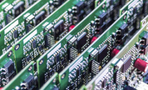
6. Thermal Management is Key
Heat dissipation is often overlooked during the design phase but is essential for maintaining the reliability and longevity of your board. Components like voltage regulators, processors, and power transistors generate significant heat, which can lead to overheating if not managed properly. Some effective thermal management strategies include:
- Heat sinks for high-power components.
- Proper ventilation around heat-generating parts.
- Adding thermal vias to transfer heat between layers.
By integrating these techniques, you can prevent your PCB from reaching unsafe temperature levels.
7. Review and Test Before Manufacturing
Before sending your design to the manufacturer, conduct thorough design rule checks (DRC) to identify potential issues. At YIC Assembly, we highly recommend running simulations and prototyping your designs before full-scale production. Testing your PCB design under realistic operating conditions will help you catch any faults early, reducing the risk of costly revisions post-manufacturing. Adopting these PCB design best practices will help you create reliable, high-performance boards that meet your project’s requirements. At YIC Assembly, we provide custom PCB assembly services to help turn your designs into reality. With expertise in various industries and access to cutting-edge manufacturing processes, we are your trusted partner for all things PCB.
 Need more advice on your next PCB design? Contact us today and let our team of experts assist you in creating the best possible solution for your project!
Incorporating these PCB design best practices will result in better performance, lower costs, and a more efficient manufacturing process. Don’t forget to bookmark YIC Assembly for your next project and stay up to date on the latest trends in PCB design!