Understanding Silk Screen Technology in Printed Circuit Board (PCB)
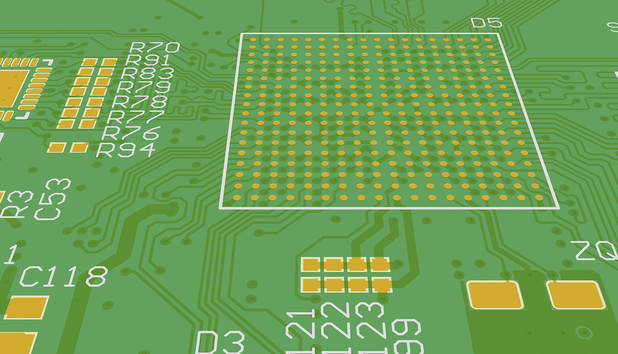
Adding the silkscreen layer onto a printed circuit board is the final step in the fabrication process. Silkscreen is a layer that uses ink traces to identify all the PCB board components, test points, parts of the PCB, warning symbols, logos and marks etc. These shapes, numbers, and letters really aren’t some new language. They can also communicate the function of each of the pins. This silkscreen is applied on the component side; all though you may find the use of silkscreen on the solder side is also not uncommon, which will increase the cost. Essentially a detailed PCB silkscreen will benefit both the manufacturer and the engineer to locate and identify all the components.
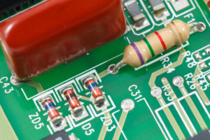
The ink that is used is a non-conductive epoxy ink. The ink used for these markings is highly formulated. There are 3 standard colors that are normally used, which include black, white and yellow, but silkscreens can be any color. If you take apart enough electronics, you are bound to find PCBs with gray, red, and even blue silkscreens. PCB software also uses standard fonts in silkscreen layers, but you can choose other fonts from the system too. For traditional silk-screening you require a polyester screen stretched on aluminum frames, a laser photo plotter, spray developer and curing ovens.
 There are three basic ways to apply silkscreen.
- Manual Screen-printing
- Manual screen-printing is done when the line widths are greater than 7 mil (0.007”) and the registration tolerance is 5 mil. For this method you require a stencil of the text and traces made of nylon. The ink is pushed through the stencil onto the laminate. Next the board is baked in a curing oven for the ink to cure.
- Liquid Photo Imaging (LPI)
- This method is used when the line widths are greater than 4 mil. Liquid Photo Imaging is quite like the process used for the application of solder mask. In this a liquid photo-imageable epoxy is coated on to the laminate and then exposed with UV light. After this the board is developed and cured. It is much more accurate than manual screening.
- Direct Legend Printing (DLP)
- DLP is the most accurate of all these processes but is more expensive. In this process an inkjet projector is used with acrylic ink that is applied onto the raw PCB directly from the CAD data. The ink is cured with UV light as it is printed. It should be noted though that the acrylic ink does not cure on boards with silver finishes.
New customer special discount on 2 & 4 layers printed circuit board fabrication. Trust our high-quality standard is the main reason we always have return customer. ACME Printed Circuit Board Assembly has over 25% customers are over 10 years relationship.
Over 25 years in the printed circuit board assembly service business, ACME Printed Circuit Board Assembly knows how to making customer satisfy, check out our Business Hall of Fame Award.
Looking for a new PCB manufacturer? Contact Yun Industrial ACME PCB today.