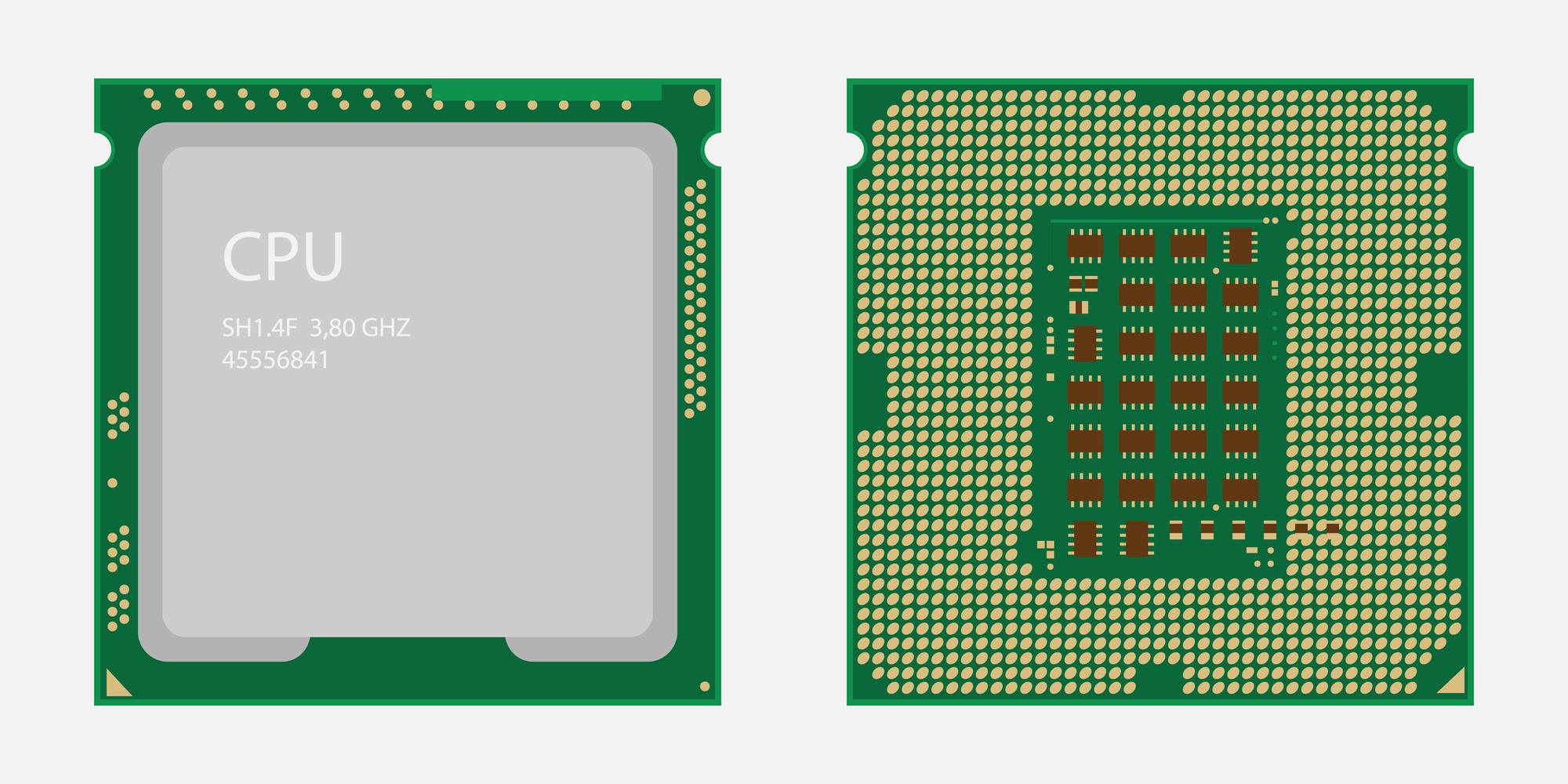
Are you looking to reduce the size of your chip carrier while enhancing its functionality and performance? Ball Grid Array (BGA) packaging may be the solution you need. As a widely adopted surface mount technology (SMT), BGA is becoming increasingly popular in modern electronics manufacturing for its ability to maximize connection density and optimize PCB layout.
What Is Ball Grid Array (BGA) Packaging?
Unlike traditional packaging methods that place pins around the perimeter of a chip, BGA uses the underside of the chip package to house a grid of solder balls. This allows for a significantly higher number of interconnection pins, leading to improved electrical performance and more compact designs.
BGA not only reduces the package size of chip modules but also enables manufacturers to design thinner and lighter printed circuit boards (PCBs)—a critical demand in today’s compact electronics market.
Types of Ball Grid Arrays
There are three main BGA types, each with its own advantages and limitations:
1. Plastic Ball Grid Array (PBGA)
✅ Low cost
✅ Excellent electrical performance
✅ Good thermal compatibility with PCBs
⚠️ Sensitive to humidity
2. Ceramic Ball Grid Array (CBGA)
✅ Superior heat dissipation
✅ High packaging density
⚠️ Expensive
⚠️ Poor thermal compatibility with PCBs
3. Tape Ball Grid Array (TBGA)
✅ Excellent thermal compatibility
✅ Best heat dissipation
✅ Lowest cost
⚠️ Sensitive to humidity
⚠️ Lower mechanical dependability
Why BGA Requires X-Ray Inspection
Since the solder joints in BGA packages are located beneath the component and not visible to the naked eye, X-ray inspection is essential for ensuring board quality. This advanced inspection process can detect critical defects such as:
Voids (gaps in the solder)
Short circuits
Missing or misaligned solder balls
Proper inspection guarantees the reliability and integrity of BGA assemblies, particularly in high-performance and mission-critical applications.
BGA vs. Quad Flat Pack (QFP)
Compared to quad flat pack (QFP) styles, BGA offers:
Better electrical and thermal performance
Higher pin density
Smaller footprint
Reduced risk of bent pins
For manufacturers seeking more efficient use of PCB space and superior performance, BGA is often the preferred packaging option.
BGA Assembly Expertise Since 1994
At YUN Industrial/ACME PCB, we’ve been offering BGA packaging and assembly services for over two decades. Our team is equipped with state-of-the-art X-ray inspection systems and deep expertise to ensure high-yield, defect-free BGA assemblies for your project.
📞 Contact us today to learn more about how BGA can benefit your PCB design and manufacturing needs.


